Products
- Multilayer PCB[10]
- Double-Sided PCB[10]
- Single-Sided PCB[10]
- Rigid PCB[8]
- Other PCB & PCBA[7]
- FPC[7]
Contact Us
- Contact Person : Ms. Lee Coco
- Company Name : Meizhou Dingtai P.c Board Co., Ltd.
- Tel : 0086-755-23325159
- Fax : 0086-755-23325496
- Address : Guangdong,Meizhou,AD Nine District, Dongshen Industrial Zone, Meizhou,Guangdong
- Country/Region : China
- Zip : 514021
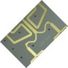
FPC PCB board for LCD
Product Detailed
Related Categories:Other PCB & PCBA
1 ,PCB manufacturer
2 ,Quick delivery
3 ,Free sample before production
4,Certificate: UL,ISO,SGS
5,Sample within 3 days
| Item | Technology for production capability |
| Surface finish | HASL/Lead free HASL/Ni gold plating/Immersion/Golden finger/OSP/Carbon ink |
| Max PCB Size | 600mm*600mm |
| Min PCB Size | 5mm*5mm |
| Tolerance for Bow and Twist | single layer≤1.0%,double layer≤0.6%,multilayer≤0.6% |
| Min board thickness&Tolerance | 0.2mm±0.08mm |
| Min Line Wide/Line spacing& Tolerance | HASL:0.10MM±20%(4mil±20%) Gold Board:0.075mm±20%(3mil±20%) |
| The distance between the copper and board edge | 0.5mm(20mil) |
| The distance between Hole edge and board edge | 0.3mm(7.87mil) |
| Min hole diameter&tolerance | 0.2mm±0.076mm(12mil±3mil) |
| copper thickness in the hole | 20-25um(0.79-1.0mil) |
| hole location devation | ±0.076mm(0.3mil) |
| Min diameter for the round hole(punch) | Board thickness for FR-4: less than1.0mm(40mil)1.0mm(40mil) Board thickness for FR-4:1.2-3.0mm(47mil-120mil)1.5mm(59mil) |
| Min diameter for the square slot(punch) | Board thickness less than 1.0mm for FR-4,CEM-3:0.8mm*0.8mm(31.5mil*31.5mil) Board thickness1.2-3.0mm(47mil-120mil) for FR-4,CEM-3(47mil-120mil):1.0mm*1.0mm(40mil*40mil) |
| Silk screen circuit devation | ±0.076mm(0.3mil) |
| The tolerance for route | CNC:±0.1mm(±4mil),Punch:±0.15mm(±6mil) |
| The tolerance for V-cut | ±0.2mm(±8mil) |
| Type | Double layer,multilayer,aluminum,ceramic,PTFE |
| Material | Fr-4,CEM-1,CEM-3,High frequency board |
| Processing thickness | 0.2mm-3.5mm |
| base copper thickness | 18um,35um,70um |
| Min hole diameter | 0.25mm |
| Plating thickness | gold plating:2.5-5um Au0.05-0.1um Immersion gold:Ni5-8um Au 0.08-0.12um Golden finger:Ni2.5-5um Au0.08-0.12um |
| Production Capability | 30000 squremeter/Month |
| Outline | CNC,punch |
| V-cut angle devation | ±5° |
| Material thickness'range for V-cut | 0.6mm-3.2mm(15.5mil-129.58mil) |
| Min spacing of SMD | 0.33mm(12mil) |
| Min clearance of solder mask | 0.076mm(0.3mil) |
| Min solder mask bridge | ±0.076mm(0.3mil) |
| Cut lamination→Drilling→Deburring→Desmear→PTH→Dry film→Imagine transfer →Plating→Eching→Solder mask→Silk screen→Surface finish→Punch/CNC→V-cut→Cleaning→E-Test→Visual inspection→Packing→QC→FQA→Shipment | |
FPC PCB board for LCD


